
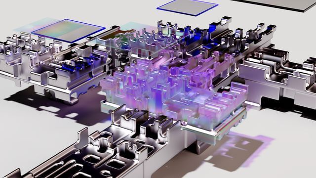
Nvidia and TSMC Enter Production of Silicon Photonics to Replace Copper in AI Data Centers
Silicon Photonics Optical AI Computing technology officially entered volume production on October 14, 2026, as semiconductor manufacturing giant TSMC confirmed commercial output of its Compact Universal Optical Engine (COUPE) platform alongside Nvidia’s Spectrum-X Photonics networking hardware. Led by breakthroughs from photonic hardware pioneers Lightmatter, Celestial AI, and Ayar Labs, the global semiconductor industry is shifting from traditional copper electrical interconnects to integrated laser light channels inside AI data centers. This architectural transition addresses severe physical energy bottlenecks, enabling hyperscale cloud providers to interconnect tens of thousands of GPUs while cutting optical power consumption by up to 70% per port.
How Much Energy Does Silicon Photonics Optical AI Computing Save for Enterprise Data Centers?
Traditional microprocessors rely on copper wiring to transmit electrical signals across circuit boards, generating massive heat and experiencing severe signal degradation at speeds exceeding 800 Gigabits per second. Silicon Photonics Optical AI Computing solves these physical barriers by integrating microscopic laser waveguides directly onto silicon dies, transmitting data via light photons rather than electrons across hyperscale AI clusters.
                  Photonic AI Interconnect Architecture
┌────────────────────────────────────────────────────────────────────────┐
│                      Co-Packaged Optics Engine (CPO)                   │
├───────────────────────────┬───────────────────────────┬────────────────┤
│ Electrical Silicon GPU    │ Integrated Laser Engine   │ Optical Fiber  │
├───────────────────────────┴───────────────────────────┴────────────────┤
│                Lightmatter Passage & TSMC COUPE Platform               │
└────────────────────────────────────────────────────────────────────────┘
The economic and operational advantages of transitioning from copper wiring to photonic light chips include:
- 70% Interconnect Power Reduction: Standard pluggable optical modules consume approximately 30 watts per interface, whereas Co-Packaged Optics (CPO) architectures reduce power draw to 9 watts per interface, saving gigawatt-hours across 100,000-GPU clusters.
- $32.19 Billion Market Projection: Financial data from SNS Insider indicates the global silicon photonics market grew from $3.02 billion in 2025 toward a projected $32.19 billion by 2035, compounding at a 26.70% annual growth rate driven by hyperscale AI compute infrastructure.
- 1.6 Terabit Transceiver Scale: Optical hardware manufacturers ramped high-volume production of 1.6 Terabit-per-second transceivers in 2026, doubling bandwidth capacity for AI model training clusters compared to 2024 standards.
When Will Silicon Photonics Optical AI Computing Achieve Mass Market Adoption?
During the third quarter of 2026, foundry and hardware manufacturers achieved critical commercial milestones across global supply chains. TSMC’s COUPE platform integrates optical engines directly with advanced chiplet packaging (CoWoS), while Nvidia began shipping engineering samples of its Quantum-X Photonics InfiniBand switches to cloud infrastructure providers like Lambda.
- Ayar Labs TeraPHY Scaling: Ayar Labs completed a $500 million Series E funding round at a $3.75 billion valuation in 2026, establishing a 1,024-accelerator reference design in partnership with Wiwynn to commercialize in-package optical I/O.
- Lightmatter Passage Platform: Lightmatter deployed its Passage photonic interconnect system across Mountain View validation labs, demonstrating laser-driven scale-up topologies that eliminate circuit board copper switches entirely.
- CPO Market Penetration: Market data from TrendForce reveals Co-Packaged Optics penetration will scale from 0.5% of AI optical modules in October 2026 to over 35% by 2030 as data centers exhaust local electrical grid capacity.
Comparing Silicon Photonics Optical AI Computing to Copper Architecture, and What Is Our Take?
For decades, chipmakers extended Moore’s Law by shrinking electrical transistors down to 2-nanometer nodes. However, at sub-2nm scales, copper wires create an insurmountable power wall where over 80% of data center electricity is wasted merely moving data between processors rather than executing mathematical computations. Silicon Photonics Optical AI Computing eliminates this bottleneck by decoupling data transmission from electrical copper.
       Comparison of Semiconductor Interconnect Technologies
┌──────────────────────┬────────────────────────┬────────────────────────┐
│ Strategic Dimension  │ Legacy Copper Cables   │ Silicon Photonics CPO  │
├──────────────────────┼────────────────────────┼────────────────────────┤
│ Transmission Medium  │ Electrical Electrons   │ Laser Photons (Light)  │
│ Power Draw Per Port  │ ~30 Watts              │ ~9 Watts               │
│ Bandwidth Density    │ Limited (<800G Runs)   │ Scalable (1.6T to 3.2T)│
└──────────────────────┴────────────────────────┴────────────────────────┘
At our editorial desk, we view the commercialization of Silicon Photonics Optical AI Computing as the most consequential hardware evolution of the post-Moore’s Law era. Without photonic interconnects, hyperscale AI developers like OpenAI, Google, and Anthropic would face a physical wall where terrestrial power grids simply cannot supply enough gigawatts to run copper-connected GPU clusters. By replacing copper wires with laser light, semiconductor leaders ensure that artificial intelligence scaling can continue through the end of the decade.
(You can also read our previous coverage on Google AI data center expansion and energy demands, where we examine terrestrial power grid constraints).